You find schematic and layout files in http://www.vems.hu/files/genboardv3/ directory.
Note that you can use CTRL-F (search) to find a component by name in the PDF (not possible in the png) schematic or layout.
- v3.1
- [v3.1 schematic] in PNG format. 259kB
- [v3.1 schematic] in PDF format. 868kB. Effectively the same as v3.2 (v3.2 has some separate 5V regulators where v3.1 has L1,L2 or trace continuity from the main 5V)
- [v3.1 board top side] in PDF format. 890kB
- [v3.1 board bottom side] in PDF format. 817kB
- v3.2
- [v3.2 schematic] in PDF format. 390kB
- [v3.2 board top side] in PDF format 580kB
- [v3.2 board bottom side] in PDF format 580kB
- [chip orientation, bottom] and [chip orientation, top]
- v3.3
- [v3.3 schematic] in PDF format. 802kB Note: See Build Procedures Section Three for note on AVCC wiring (missing 33 Ohm resistor)
- [v3.3 board top side] in PDF format 1MB
- [v3.3 board bottom side] in PDF format 900kB
- v3.5
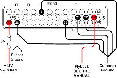
- [v3.5] layout in pdf format. The F1 throughole pads for regenerating fuse (same as R19 SMD pads) right from EC36/25 pin make the layout more suitable to use a PTC (eg. 3A 30V) for added voltage spike protection ( perhaps even some reverse supply polarity protection, but this is not guaranteed). No other changes. No schematic change at all.
- v3.6
- [v3.6] layout and schematic pdf.
- only small change is AudiTrigger/CamHALLInverter onboard, find Q13 on the schematic. Q13 is on the bottom side of the board around the middle, at the 3+2 pinheader group.
- Note that the small Q13 SOT23 NPN inverter transistor is NOT populated by default, but normally bypassed (short between base and collector).
- populated for InputTrigger/AudiTrigger when 3 triggers are in use. See [shop text] for the actually used input for your chosen HW setup
- theoretically (but almost never in practice, only if negotiated during/before ordering) Q13 can also be used for custom use eg. mcp3208 analog input pin protection when used for digital input, eg. on/off button.
![[v3.1 schematic]](http://www.vems.hu/files/genboardv3/vems_v31_r222_schematic.png)
The standard EC18 wiring (since 2009-09-29):
- [more printouts for v3.x]
- [ v3.x pin information] in PDF format. 356kB.
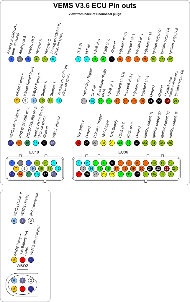
- GenBoard/VerThree/PinOut
- GenBoard/VerTwo/CircuitDiagrams has schematics for the v2.x boards
Advanced users - only for manufacturing
There are some bin/categories.* files in CVS (see GenBoard/ManuFacturing) that in some cases override component values found on the schematic (mostly supply capacitors).
FET orientation
All the TO220 switches on GenBoard/VerThree have the same orientation (at least electrically, because some people mount them below the PCB and some mount them above).
- S (source) is the GND5 for all switches
- D is the switched point that goes to EconoSealIII connector (this point jumps to several 100 Volts when ignition transformer is driven by IGBT, so it can kill you ! Similar thing happens if you forget about injector FlyBack, but that usually kills the FETs before you)
- G is the gate, which controls the device. There is always a resistor before it (usually 22 ohm installed for PWMing setup, and 1000 Ohm for nonPWM-ed FETs and all IGBTs) and some controlling device (like AVR, FETdriver or ign259 chip). The diodes parallel with the IGBT gate resistors are not necessary.
But you see this on the schematic anyway.
See also