Changes by last author:
Added:
|
This is an obsolete page is for HW developers: about the design of a custom CNC case solution.
There are some new case designs that are manufacturable and cost efficient. The maintenance is in another (non-fully public) wiki, for easier communication with manufacturing partners, and protection of some files that are not our own property (designed by partners: partners usually don't allow their design being manufactured by their competitor's). If you want to work on it, contact MembersPage/MarcellGal or MembersPage/JörgenKarlsson for access. The Alubos case and v3.x is professional, and works very well, see GenBoard/VerThree/CaseAndMounting v3.3 will probably stay TO220 (TO220 FET inventory is huge) but ARM boards would be DPAK For future boards there would be advantages of a partially CNC-ed case: * case manufacturing and environmental costs (this is already acceptable with alubos1600 + frontplate + endplate design) * assembly costs (could be improved) * chance to measure signals inside and service without disassembly (just remove top, while bottom stays and cools). ---- Alternatives? We also need to look into available cases. Maybe some Ford or GM uses a suitable cheap case that is available brandnew and also from junkyards. This is rather for the ARM series (than v3.2), that is rerouted anyway. Maybe a case that was originally designed for other applications is available and suitable. ---- choices for case manufacturing technology * brute-force (negative approach): take a big block and machine away the internal. Given the frontplate files, it shouldn't be more than 40 hours to design. Environmentally unfriendly, and relatively expensive. * positive approach (molding, casting, whatever it's called) takes slightly more refined design than only machining, but more environmental-friendly and eventually cheaper * 3 pieces: starting from appr. 25..35mm slices of (eg. rectangular) extruded profile, see below for some known to be available sizes, most are metric. SMD DPAK switches on the bottom of the board. ** bottom from finned offtheshelf Al profile (yes, available, see below; cutting is very environment friendly, unlike milling). ** The top would be 3mm Al plate (plexi for demo versions). Both bottom and top would have shallow 0.5 mm milling at circumference for aligning (this is also fast). Either top, or side would need some milling for the chosen connector, but this part is fast. Although this method is 3 parts not the minimal 2, but all 3 parts are very environment-friendly and assembly is not an issue. After spending a few days near machining stuff and consulting expert machinists I'm very much biased towards this. Check profiles below. The board is screwed at the corners to the bottom lid. The four TO220IGBT's is clamped to the profile. Something like this:
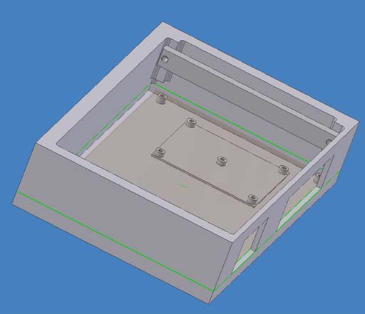
The thick walls is only there to visualize the outer dimensions. I'll make fins and mounting ears along the edges. ---- Available rectangular (hollow) profiles The use of a profile cuts material cost and saves environment. * 104X164mm internal profile (from where ??) * 4"x6" (external?) (from where ??) * outerX x outerY x wall (mm) (metalloglobus.hu items: ) * 60x60x3 * 80x40x2.5 * 80x50x4 * 100x50x3 rectangular (6m pieces, 1838Ft+VAT/m, AlMgSi0.5). We will cut this on the 50mm side to our needs. If we are lucky, 100x24.5 and 100x24.5 mm is enough (but prolly not enough because of EC height - maybe with seal?). We can cut to 100x30 and 100x18mm and save the 18 mm for some non-EC application later (flying loom VemsFrontier/ArmUfo ?). The internal width is 94mm (100-2*3mm) which determines max PCB width (90..93 mm?). * 120x30x2.5 * 100x50x3 This would be good for several smaller boards, even ones with display. A bit small for a full-featured ECM with bloated connector. Available U profiles: * 60x40x4 U profile: not wide enough for EC36 or other if we want >500kg ---- Available one-side-flat fin-profiles SMD switches on the bottom of the board, touching the flat side of the fin-profile. Each DPAK can dissipate > 8W this way, could someone confirm this? * width x (min .. max height) ..... (metalloglobus.hu items: ) * 125 x (10..50) with 10 fins * 111.1 x (7.4 .. 32.7) with 14 fins This is very nice.(itemnr=8261. 3m pieces at metalloglobus.hu ). The 7.4 mm measures 7.6mm - not that it matters. * 96 x (15..60) with 7 fins ---- Extruding custom profile First I thought this is over our budget. But it seems it is possible to order from just 500kg of Al. That is about 1000 cases (depending on what thickness we want for the finned part), for appr. the price of 300 Alubos cases (1600 or 1000 series, similar price). Note that there are 2 ways to do this: * self-mating U profile that is used for top and bottom (endplates are like for v3) The 2-part 100mm wide Alubos (ABPH1000?) is almost good shape to start from (but alubos has no fins, and expensive). Note that PCB must be bolt-to-bottom (so the SMD DPAK-s on the bottom touch-up) rather than slide-in. Matching frontplate and endplate is a must, but not a big deal :-) * rectangular profile (that makes the sides). Bottom cap is offtheshelf finned (-cut), top is standard 3mm plate. This would be best to buy off-the shelf somewhere between 100x80 .. 120x90 mm size. In either case, some fins are nice for cooling. ---- Specifications for Custom Case: * Closed bottom * Smooth interior * Min. 3..4 mm fins at the outer side, close to where switches touch ---- Brain Storming Area: The econoseal limits the min height of the box. When analyzing the requirements I found that we can make a nice utilization of the material if we mount every dumb thing on the bottom of the board: * SMD switches (FET's, IGBT's) * EC36 and EC18 * header connectors All smart things go to the top (as now). This way we can cut the case, so there are deeeeep cooling fins under the swithces (all the height coming from the EC requirement can be utilized as fins). And servicability remains, we can reach all the smartees with scope probe while swithces are cooled. Unfortunately the wires going to the headers are not easy to change that way. Ideas? Need to rubbermount case to vehicle? -- As long as we provide 'lugs' to bolt through its down to the installation as it how it's mounted. Rubber mounts will insulate the case from the car chassis. [PhatBob] ---- The solution to that would be to scale down a bit to a smaller standardized size (half?), and have several units, each of which are less functionality than v3, but with superior interconnection (each having ARM and CAN). Togo: GenBoard/VerFour is talking about a CPU on a pluggable board doing that right could half the Board size and standardizing this well could give us the options of faster design changes (I know the connector fear... but given good quality Gold plated contacts in this hermetically sealed enclosure ?) Alternatively the option exists to use instead of the thruhole connectors flat Band cable and then (while movement is minimized) there is no connector problem anymore ... Of course we have to place the mounting holes more to the inside so a modular cpu board can be mounted on studs that extend through the Bottom power and sensing board. The Cpu Board has to be that much smaller so it keep clear of Power transistors or other high profile components (connectors etc) Is there a SealedConnectors Page to discuss any options we may have: I am specifically thinking about the 1mm Econoseal maybe an option if we want to shrink the whole controller! - Tobias ---- Good side: * mounting the SMD switches is easier * the case top could be removed while the switches are cooled (by being fastened to the bottom) so any measurement or improvement could be done on the top side * it would be absolutely awesome * no supply-chain issues (as with the Alubos) Bad side: * manufacturing gaskets would be tough -- It would be easy enough to machine a channel that will locate a neoprene/rubber 'o-ring' type material to act as a gasket, making a gasket would be a case of cutting the rubber to the right length and a dab of silicon. [PhatBob] * only one circuit in a case would be supported It is possible to design and manufacture the board and CNCed case in about 4 weeks, but we need to select (and order!) the SMD switches as soon as possible, as that takes a lot of time. * SMD clamping IGBT - IRGS14C40L (someone verify please) * SMD logic level FET - RFD16N05LSM (Really unsure on this one, please check) Seems a little expensive though at US$0.527/1000 * SMD vanilla FET (might not be needed, if we use the logic level everywhere) Jörgen, I count on you in this. ---- *A prototype of the Case: [VEMS Case] Lacking heatsinks for SMD switches and correct Ecnoseal position, probally needs thicker walls for gasket. Have heatsink for the PSU of Genboard and MAP sensor mounted underneath board. ---- Tobias: How about this one: I don't know what it costs to cut it out of one solid block of ~170*150*40mm? -- Machining costs are often more costly than the price of the materials. [PhatBob] As I hear 60..100 USD / hour are normal machine costs. Definitely we want as shallow as posible (but if we go with the 2 big-piece design, that means at least 32 mm heaight to be machined, for the 160x100 mm block). I think the Powertransistors should have gone more along the long sides. Now I think that * all FETs and 4 IGBTs must be SMD on the bottom of the board * Econoseal 18 and 36 mounted on the BOTTOM side of the board. Yes, that breaks pinout compatibility * header pins mounted on the BOTTOM side of the board. Yes, that breaks header pinout compatibility * 4 IGBTs should be TO-220 on the right side of the board * the case-bottom is thick so it houses the Econoseal. ** On the right side the case-bottom has flat surface on the inside relatively high to touch the SMD switches, and deep cooling fins on the outside (CNC-ed with big, fast moving tools). ** On the left side much of the case-bottom is machined away so the header-pins are housed - there is a step inside near the middle that makes this possible. ** Also, there is a plateu on the right side of the case-bottom (another step) that helps clamping the 4 TO220 IGBTs on the right. Yes, this 15 mm adds to the 160mm :-( * the case-top is relatively thin, not much material to move away. But removing the case-top makes it possible to measure the interesting signals on the top of the board without disturbing cooling. Please confirm that it is is clear without a drawing how that would work. Can someone draw? Tobias: Sounds like major redesigning of the PCB is necessary anyway. (I wouldn't call that major, as the right side is only 1/10 work compared to the left side, and 1/50 of the work that was already spent on the board till now - which includes reworks). I don't share your visualization of what you expect to gain from flipping the connectors to the bottom side? I do understand it in the Kontext that you want to keep more material and use it for cooling fins... exactly But then how are you going to clamp the To220s if they are not accessible on top ? They are accessible. That makes the +15 mm in the 160 mm direction. SMD Power transistors should still go to the edges of the board, (NO!! rather to the bottom! Also note that FETs wouldn't need to touch anything for cooling at all.) If the manufacturing costs are really that high we should investigate (once the design is stable) who can do casting and molding and how the pricing for that would be ... meanwhile I guess beside the new PCB a drawing will be necessary! That is a good idea, search for backyard metalcasting, and look for shops that do it. For 100+ pieces it is very good option, but the design is more complex than for CNC-ing. http://www.vems.hu/files/misc/GemBox01ViewsW-small.jpgI designed this one with Metall Pressure Casting in Mind... Tobias: Apparently there is no straight Econoseal connector? Would be flatter and less expensive I imagine? The option of cushioned mounting, or if that isn't necessary, the suggestion to mount it with a set of bolts through the Sheet metal secured by nuts and then finally another nut on top to be able to remove and replace the controller box without having to remove the bolts? Somebody could use spacers Instead? The mounting of the transistors in future versions should be straight to the case (as it's always been in the past as well for v3.x :-) For more than 10A current the TO220 transistors can be distributed in straight lines along the board edges with their mounting surface facing outward. For max 10A current SMD switches should go to one side of the PCB, and simply the PCB is attached to the big flat bottom of the case so the SMD transistors are heatsinked nicely. We should as soon as possible come up with a sufficient bolt pattern for the bottom. The above 2 can be combined. BPoindexter: We have a custom machine design/build shop. I would like to contribute to the design/machining of custom case of CNC machined billet variety. What would be next steps to get prototype going? ---- And here is the next version of the case based on the suggestions on this page -
This is the lowest cost design (fewest machine operations), its a first cut so I would appreciate feedback as to how we can develop this further. * I think changing some angles would make it more mold-friendly * more bolts * The mouting flange has to go to the other side so it complies with the design requriments. [PhatBob] Other side do you mean at the top? * It also lacks the SMD cooling Fins on the Outside of the case Read at top of page.. [PhatBob] This is true but without the SMD dimensions I can't finish the heat sinking. Most of the OEM cases that I've taken apart sink heat to the case without needing cooling fins, are we really going to need them? I ask this as I'm not an expert but I know that there is a lot of aluminium there. Heat sinks do have that 'bling' factor and that sells product (so I aint against it!} * It also needs the skip the 25 radius between flange and wall of box because of complexity of CNC milling vs function (If one does Automated CAM generation it makes the files slightly larger but costs neither time nor gives advantages to make the thing dangerous (sharp edges) [PhatBob] I was thinking of Using a ball nosed cutter along this part, if the flanges are on their way out then we dont need to worry about this at all * there's no need to mill away that much material near the screwholes. Longer screws are OK, and cooling fins can be machined there instead of milling away everything. * 4 Bolt Holes are enough for a 100*160 Board ??? * Is there a Bottom part? [PhatBob] Not yet I drew this up the day before my holiday so that I could consider what needed to be done for the bottom, also the design is not finalised so it maybe that the case needs to take the board upside down in relation to where it is now. * Somebody explain to me how the power transistors are bolted to the metal with the PCB in the way? [PhatBob] a peice of aluminium will sit in between the rows of power transistors. threaded holes at the sides will transistors provide fastening for the transistors, and a couple of threaded holes on the top will allow a counter sunk screws to be used to fasten the block to the case. I did not put this into the drawing as the SMD transistors will make mounting different. Tobias: That brings me to the idea why not have just the power components on their own PCB (Even with their own Power-Econoseal to the Outside) and just a few flexible wires (or flat cable) to the control board. This would contribute to be able to mount the transistors more directly and permanently (with heat transfer paste) to the case and having an additional level of PCB will allow to reduce the Box size ! As I said modularization also helps to accelerate the Project evolution by allowing to leave any satisfying part unchanged for longer! ---- BPoindexter: I would recommend getting rid of the flanges, instead have mounting holes in flat base cover. The fasteners that mount board could serve to also mount base cover to main box. [PhatBob] The flanges serve for locating the box during machining, this way a jig will not be needed. The fasteners that mount the board will fasten the bottom of the case. Also, where possible, design with largest radii in mind: larger radius = larger end mill = less cut time = less $. One [PhatBob] Roughing will be done with a large cutter, then a 2.5mm rad cutter is used to machine the corners. The 5mm dia holes that give a square relief in the corners are drilled before cutting. example question, does board need to have square corners or can it have radius (or chamfer) to fit cavity with radiused corners? If this is too confusing w/o a drawing, I can have a [PhatBob] The board comes with square corners, its easier to make reliefs than to change the board design revision tomorrow. What file format is your model? We use Solid Edge - hopefully can import your file and save design [PhatBob] I use SolidEdge v9, I also have a friend who will let me do the machining for cost if I write the program, which is what I usually do, I'll probably do a couple from offcuts which I can pass onto the developers free of charge. An example of my previous work can be seen on my members page. time. I understand cooling fins are necessary/desired. Once a design is agreed upon, the first prototype lot could be run within a few days. What is the prototype lot quantity? Who are the players for review? Some input would be helpful. Thank you. Note that the VemsFrontier/ArmEfi dimensions and layout (including DPAK placement on bottom) are basically fixed. ---- [!fred]Seems to me that the dimensions are going to be tight, and just to fit the VEMS board. This project is in one way an experimenters project, and i for one would like to piggy back another board with other functions within the same enclosure, talking to the vems via SPI bus. What comments are there on what available space will be left?. I suppose there are 2 competing sides - one wants the box as small as possible, the other doesn't care so much.Please consider this guys. [Rich] How water resistant will this design be? It's a factor for us 4wd guys, and also for any motorbike folks. Is there provision for sealing, or will it need silicon? In reply to fred, I suspect the bike guys will want a small case too... can the keen experimenters not DIY with their own more suitably sized box? Any case we put effort into must be sealed - otherwise it would be a waste of time. I consider it acceptable if it requires some silicon (eg. around the connector and where the top-cover meets the box). ---- Links * http://www.big-box.hu/ceginfo/ makes sheet-metal (IMHO junk-looking) cases like many factory ECMs |

![[VEMS Case]](http://www.vems.hu/files/MembersPage/JohanEriksson/Box.jpg)