This is just to look at if an ARM processor can be subsituted for the current AVR processor
A bit obsolete since it builds on the LPC2129 processor that is unlikely to be used - in favor of AT91SAM7A3
I was at a Renesas / Atmel ARM / Atmel AVR technology day today. Not much new, it just confirmed what we already know (and let meet some people).
- it is a good decision to use known family (that is AVR for us, eg. atmega88/atmega168) for small footprint designs
- for feature-rich designs it sounds like a good way to jump from 8 bit directly to 32 bit: namely ARM. The price makes it very feasible (total system cost can be even lower if you consider the rich peripheral set)
- Renesas (although a respectable family, near Atmel and Texas height; 2 levels above microchip) did not really steal my heart
- AT91SAM7A3 EEPROM is nonexistant. Some firmware smarties are needed to store config and tables in flash with reasonable flash-life expectancy: no full page write immediately in every case a variable is updated. Needs more study if firmware operation is not disrupted while flash is being written (including interrupt vectors, whatever).
Developers found that
- v3.x IO is too powerful
- 160x100 mm size board is a bit big
- the TO220 switches makes manufacturing a bit expensive (we like DPAK)
- the smaller size board needs redesign with modified CaseAndMounting in the main focus
- CAN communication ports must be added
- max232 can be dropped (we can stock FBUS cable)
While v3.x will be manufactured as the most powerful (output count + current) board for a long time, a set of smaller, more modular boards with champion network capabilities are being designed: see VemsFrontier/Boards and VemsFrontier/ArmEfi
6/17/04
Worked with Jorgen on the mapping. Turns out that the ATMEL AVR board has 4 timers, and the ARM only has 2. I tried to add 2 UARTs, 2 SPI, 2 CAN, and still have enough for the PWM outputs.
no joy. The firmware folks need to decide how they are going to use the MAT, CAP, and PWM I/O ports with only 2 timers available.
With only. 1 UART, 1 SPI, 2 CAN, there are 4 PWM outputs out of 6 free.
We definitely want to add 2 CAN transceivers (maybe the Microchip ones), since this is a major target for the new board (so it can communicate with distant brothers that collect signals or drive whatever so the total output count for a multiboard system can easily go above 100 and the input above 60...).
No question we need the special supplies for the ARM. Maybe we will have several SOT89 supply regulator chips. (that was the plan anyway, to drop the LM2940S and put on several smaller ones, either MC33269DT (800 mA) or only some SOT89 (100mA each) is well enough if there is separate one for digital 5V, analog 5V, 3.3V, keyboard, etc...
drop candidates (when lacking space or ARM IO):
- mid OPA (we lose 4 ADCs anyway, so this is of little use)
- 2 extra FETs -- I want to keep these(Jörgen)
- the 2nd LM1815
- knock (especially if ION can somehow get on, but Jorgen wants it separate from the fuel FETs, he might have some reason) --I want to keep knock on main board (Jörgen)
- EGT (not much space there though)
- stepper
- Only leave 2-4 of the ignition channels. --Jörgen
What about this...
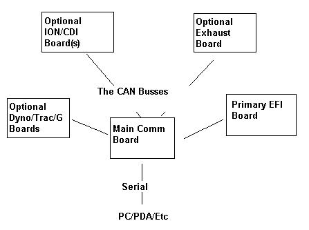
In light of tight resources and versatility, which are most important, I think I have come up with a solution which could really help out with the way we do engine management. Below is just a rough diagram of how we should break stuff up.
Economical and Versatile Reasons/Examples
Not everyone wants ION, and others want a different number of EGT and Wideband O2 then the next guy. We could offer 4 different "Optional ION/CDI Boards". Example: ION inputs for cylinder configuration of 4, 6, 8, and a custom ordered unit. Data will be sent using the CAN Bus both ION voltage and timing adjustment signals should be sent.
This also makes sense for what I listed as "Optional Exhaust Boards." These would offer us Wideband 02, EGT, and knock sensor inputs. Exhuast boards could be ordered with common configurations and then custom orders. Data will be sent using the CAN Bus.
For the Dyno/Traction/G Board, the only thing that would really assist the economical reasoning is an optional ABS controller for traction control and stability management.
The main board is where things begin to shine. Since all optional boards contain a CAN Bus, this layout would have the mainboard recieving sensor data and calculation outputs for use by other boards and for data logging purposes. The mainboard could also contain the configuration tables for the mainboards. The subboards could periodically update their tables from the mainboards table.
This mainboard could give us some free resources for unique interfacing.
- A nice LCD ouput
- Keyboard Input
- Ethernet output to host a webpage for a multiplatform compatabile configuration managment and downloading of data logs. The data could be organized as files and displayed through the web browser as a generic delimetted file and then cut and pasted into excel or whatever.
- The list continues.
System Example
Jörgen
For me it?s very important that everything can work as a standalone unit. The word 'mainboard' makes me shiver. But I think that the communications board is a good idea. That way we could let the advanced communication stuff like keyboard, LCD, USB, Ethernet, Bluetooth, on board logging (MMC) and web interface would not have to be implemented on the other boards.
Serial RS232 communication must definitely be implemented on each and every board. Using a CAN to RS232 adapter is not acceptable.
The specifications for ION say that it is made for four cylinders and you add as many as you need. The EFI board will support simple ignition in addition to it's injection capabilities. Engine board will add many temperature sensor inputs and also provide two additional WBo2 inputs in addition to the stepper driver and high current drivers. The traction control board handles traction control and logging of chassis parameters.
It's important not to force anyone to pick up a board he don't want to be able to use the one he wants. For example if someone want traction control he should be able to use it with his OEM engine management if he want that. ION is probably the one that is most important to get working as a standalone unit or as a smart ignition module for OEM or aftermarket enginemanagement systems. The only one that does not need to be generic enough to work with other brand products is the EFI board which is standalone by nature.
Frank
I see what you are getting at. The reason for dividing things up like that is because I am under the assumtion that CAN Busses cant support more then 1 device besides the host. Is this wrong? If so, then great. The proposed Mainboard and EFI board can be combined with the exception of user interfacing. I still think a "common pool" where all boards put information is needed. All boards can pull information from there, including the user interface. That way if we add a board for some reason, we can have 1-2 less items that need updating with new firmware.
If CAN can support more then one item, then that makes sense in regards to Ionsensing boards... if 4 cylinder, then one board... if 6-8 cylinders, then 2 boards. I still think that we need to look at the proposed exhaust board a little closer. Maybe just offer two boards... 1EGT/1WB02/1KNOCK and a 4EGT/1WBO2/1KNOCK. Most will want the 1/1/1 while the crazy people will want 1 or 2 of the 4/1/1 for 6 and 8 cylinder setups.
Have you seen GenBoard/EngineBoard?? -ERGH!!! I have been playing catch up, missing alot of stuff.
Basics.
- Does the part fit in the current footprint?
- close enough
- What are the types of I/O on the current AVR
- see below
- What signals are required to be mapped
- see below
- Port A -- Is used for driving the injector ckts either High Z or Low Z (normal I/O, no alternate)
- Port B -- Uses all the alternate uses for compares of PWM(guess) PB4-PB7 and the SPI ports PB0-PB3
- Port C -- Is used for driving LCD(PC7-PC4, PC1, PC0), and Knock(PC3,PC2)
- Port D -- mixed?
- Port E -- all specialized
- Port F -- all for ADC
- Port G -- all normal?
---
- Questions to be answered, that have been identified today.
- two types of UARTs, one provides full modem handshaking (8pins), and one provides only Tx/Rx (2 pins)
- 2 CAN controllers
- Serial I2C
- SPI serial I/O controller
- ARM only has 4 Analog to digital inputs AND they are 0..3V vs. the 8 on the AVR
- To get ONE external interrupt (EINT0..3) you must lose one of these (but who wants that? We only want 2..4 input captures - which can also fire interrupt of course)
- EINT0 -- RXD0 UART0 or PWM3
- EINT1 -- SDA (I2C clock I/O) or MAT0.0(Match Timer 0 channel 0)
- EINT2 -- SSEL0 (slave select for SPI0) or PWM2
- EINT3 -- RXD1( Rx input UART1) or PWM6 this is the current selection.
Response: There are plenty of Input captures from the timers but they often do double duty
- p0.2 Capture0.0 (Timer 0) OR SCL (used already)
- p0.4 Capture0.1 (Timer 0) OR SCK0 (used already)
- p0.6 Capture0.2 (Timer 0) OR MOSI0 (used already)
- p0.10 Capture1.0 (Timer 1) OR RTS UART 1 (Free)
- p0.11 Capture1.1 (Timer 1) OR CTS UART 1 (Free)
- p0.17 Capture1.2 (Timer 1) OR SCK1 or MAT1.2 (Match output Timer 1 ch 2) (Free)
- p0.18 Capture1.3 (Timer 1) OR MISO1 OR MAT1.3 (Free)
- p0.19 Capture1.2 (Timer 1) OR MAT1.2 OR MOSI1 (Free)
- p0.21 Capture1.3 (Timer 1) OR PWM5 (Free)
- p0.27 Capture0.0 (Timer 0) OR MAT0.0 (Free)
Please understand that input capture is an enhanced kind of external interrupt, that besides starting an interrupt handler, also remembers the exact time when the input changed.
Match0.0 ( Timer 0)
Match0.1 ( Timer 0)
---
New Power supply requirements for the ARM
- Power supply stuff
| Vss | GND 0V reference | 6, 18, 25,42, 50 | ||
| Vss A | Analog Ground | 59 | (Same as Vss, but isolated to minimize noise and error) | |
| Vss A-PLL | PLL ground | 58 | (Same as Vss, but isolated to minimize noise and error) | |
| V18 | 1.8V Core Supply | 17,49 | ||
| V18A | Analog 1.8V Core Supply | 63 | Nominally the same as V18, but should be isolated | |
| V3 | 3.3V Pad Supply | 23, 43, 51 | Power supply for I/O ports | |
| V3A | 3.3V Analog Pad Supply | 7 | Analog nominally the same voltage as V3, but isolated | |
| Total Power pins | 14 | AVR power pins | 7 | net loss 7 I/O pins |
Begin mapping of the I/O
- Specialized I/O
| AVR name | AVRpin | VEMname | Signal Type | ARM map | ARM Pin | Description |
| PEN | 1 | Programming | NC | PEN is a programming enable pin for the SPI Serial Programming mode. By holding this pin low during a Power-on Reset, the device will enter the SPI Serial Programming mode. PEN has no function during normal operation. | ||
| /RESET | 20 | Programming | /RESET | 57 | Reset input. A low level on this pin for longer than the minimum pulse length will generate a reset, even if the clock is not running. The minimum pulse length is given in Table 19 on page 48. Shorter pulses are not guaranteed to generate a reset. | |
| XTAL2 | 23 | XTAL MEGA | clock | XTAL2 | 61 | Output from the inverting Oscillator amplifier. |
| XTAL1 | 24 | clock | XTAL1 | 62 | Input to the inverting Oscillator amplifier and input to the internal clock operating circuit. | |
| AREF | 62 | vref | NC | ADC Vref: AREF is the analog reference pin for the A/D Converter. | ||
| AVCC | 64 | VCC | NC | ADC VCC: AVCC is the supply voltage pin for Port F and the A/D Converter. It should be externally connected to VCC, even if the ADC is not used. If the ADC is used, it should be connected to VCC through a low-pass filter. | ||
| AGND | 63 | GND | NC | ADC GND | ||
| VCC | 52 | VCC | NC | +5V(??) | ||
| VCC | 21 | VCC | NC | +5v(??) | ||
| GND | 53 | GND | NC | Digital GND | ||
| GND | 22 | GND | NC | Digital GND | ||
| GND | Vss | 6, 18, 25, 42, 50 | Digital GND, 0V reference | |||
| AGND | Vss A | 59 | Analog ground nominally same as Vss, but isolated | |||
| PLLGND | Vss A_PLL | 58 | PLL Analog ground nominally same as Vss, but isolated | |||
| VCC | V18 | 17, 49 | 1.8V core voltage | |||
| AVCC | V18A | 63 | Analog 1.8V core voltage | |||
| VCC | V3 | 23, 43, 51 | 3.3V PAD voltage | |||
| AVCC | V3A | 7 | Analog 3.3V PAD voltage |
- Port A
- The Port A has an alternate function as the address low byte and data lines for the External Memory Interface.
| AVR name | AVRpin | VEMname | Signal Type | ARM map | ARM Pin | Description |
| PA7(AD7) | 44 | PRE INJ07 | Std I/O | GPIO00 | ||
| PA6(AD6) | 45 | PRE INJ06 | Std I/O | GPIO01 | ||
| PA5(AD5) | 46 | PRE INJ05 | Std I/O | GPIO02 | ||
| PA4(AD4) | 47 | PRE INJ04 | Std I/O | GPIO03 | ||
| PA3(AD3) | 48 | PRE INJ03 | Std I/O | GPIO04 | ||
| PA2(AD2) | 49 | PRE INJ02 | Std I/O | GPIO05 | ||
| PA1(AD1) | 50 | PRE INJ01 | Std I/O | GPIO06 | ||
| PA0(AD0) | 51 | PRE INJ00 | Std I/O | GPIO07 |
- Port B -- Uses all the alternate signal types (specialize I/O)
- Port B alternate functions are listed below
| AVR name | AVRpin | VEMname | Signal Type | ARM map | ARM Pin | Description |
| PB7(OC2/OC1C) | 17 | OC2 | Output Compare#2 | OC2/OC1C(1) (Output Compare and PWM Output for Timer/Counter2 or Output Compare and PWM Output C for Timer/Counter1) | ||
| PB6(OC1B) | 16 | OC1B | Output Compare#1 | OC1B (Output Compare and PWM Output B for Timer/Counter1) | ||
| PB5(OC1A) | 15 | OC1A | Output Compare#1 | OC1A (Output Compare and PWM Output A for Timer/Counter1) | ||
| PB4(OC0) | 14 | OC0 | Output Compare#0 | OC0 (Output Compare and PWM Output for Timer/Counter0) | ||
| PB3(MISO) | 13 | MISO | Programming | p0.5 MISO0 | 29 | MISO (SPI Bus Master Input/Slave Output) |
| PB2(MOSI) | 12 | MOSI | Programming | p0.6 MOSI0 | 30 | MOSI (SPI Bus Master Output/Slave Input) |
| PB1(SCK) | 11 | SCK | Programming | P0.4 SCK0 | 27 | SCK (SPI Bus Serial Clock) |
| PB0(SS) | 10 | SS | Programming | P0.7 | 31 | /SS (SPI Slave Select input) |
- Port C
- The Port C has an alternate function as the address high byte for the External Memory Interface.
| AVR name | AVRpin | VEMname | Signal Type | ARM map | ARM Pin | Description |
| PC7(A15) | 42 | L Bus 7 | Std I/O | GPIO08 | ||
| PC6(A14) | 41 | L Bus 6 | Std I/O | GPIO09 | ||
| PC5(A13) | 40 | L Bus 5 | Std I/O | GPIO10 | ||
| PC4(A12) | 39 | L Bus 4 | Std I/O | GPIO11 | ||
| PC3(A11) | 38 | KNOCK INTEGR | Std I/O | GPIO12 | ||
| PC2(A10) | 37 | CS KNOCK | Std I/O | GPIO13 | ||
| PC1(A9) | 36 | LCD EN | Std I/O | GPIO14 | ||
| PC0(A8) | 35 | LCD DDIR | Std I/O | GPIO15 |
- Port D -- pins PD0..PD4 obviously the specialized functions
| AVR name | AVRpin | VEMname | Signal Type | ARM map | ARM Pin | Description |
| PD7(T2) | 32 | CS P259 | Std I/O | GPIO16 | T2 (Timer/Counter2 Clock Input) | |
| PD6(T1) | 31 | CS S259 | Std I/O | GPIO17 | T1 (Timer/Counter1 Clock Input) | |
| PD5(XCK1) | 30 | CS CAN | Std I/O | GPIO18 | XCK1(1) (USART1 External Clock Input/Output) | |
| PD4(IC1) | 29 | IC1 | Input Capture#1 | ICP1 (Timer/Counter1 Input Capture Pin) | ||
| PD3(TXD1/INT3) | 28 | TX1 | UART#1 | 33 | INT3/TXD1(1) (External Interrupt3 Input or UART1 Transmit Pin) | |
| PD2(RXD1/INT2) | 27 | RX1 | UART#1 | MUTUALLY EXCLUSIVE with INT6 | 34 | INT2/RXD1(1) (External Interrupt2 Input or UART1 Receive Pin) |
| PD1(SDA/INT1) | 26 | SDA | p0.3 SDA | 26 | INT1/SDA(1) (External Interrupt1 Input or TWI Serial DAta -- ARM I2C Data) | |
| PD0(SCL/INT0) | 25 | SCL | p0.2 SCL | 22 | INT0/SCL(1) (External Interrupt0 Input or TWI Serial CLock -- ARM I2C -clock ) |
- Port E -- mixed specialize
| AVR name | AVRpin | VEMname | Signal Type | ARM map | ARM Pin | Description |
| PE7(IC3/INT7) | 9 | IC3 | INput Capture#3 | INT7/ICP3(1) (External Interrupt 7 Input or Timer/Counter3 Input Capture Pin) | ||
| PE6(T3/INT6) | 8 | INT6 | External Interrupt | p0.9 EINT3 | 34 | INT6/ T3(1) (External Interrupt 6 Input or Timer/Counter3 Clock Input) |
| PE5(OC3C/INT5) | 7 | OC3C | OUTput Compare#3 | INT5/OC3C(1)(External Interrupt 5 Input or Output Compare and PWM Output C for Timer/Counter3) | ||
| PE4(OC3B/INT4) | 6 | OC3B | OUTput Compare#3 | INT4/OC3B(1)(External Interrupt4 Input or Output Compare and PWM Output B for Timer/Counter3) | ||
| PE3(OC3A/AIN1) | 5 | OC3A | OUTput Compare#3 | AIN1/OC3A (1) (Analog Comparator Negative Input or Output Compare and PWMOutput A for Timer/Counter3) | ||
| PE2(XCK0/AIN0) | 4 | KB DATA | Std I/O | GPIO19 | AIN0/XCK0(1) (Analog Comparator Positive Input or USART0 external clock input/output) | |
| PE1(TXD/PDO) | 2 | TXD | UART#0 | p0.0 TXD0 | 19 | PDO/TXD0 (Programming Data Output or UART0 Transmit Pin) |
| PE0(RXD/PDI) | 1 | RXD | UART#0 | p0.1 RXD0 | 21 | PDI/RXD0 (Programming Data Input or UART0 Receive Pin) |
- Analog Inputs aka Port F
Port F also serves as an 8-bit bi-directional I/O port, if the A/D Converter is not used. Port pins can provide internal pull-up resistors (selected for each bit). The Port F output buffers have symmetrical drive characteristics with both high sink and source capability. As inputs, Port F pins that are externally pulled low will source current if the pull-up resistors are activated. The Port F pins are tri-stated when a reset condition becomes active, even if the clock is not running. If the JTAG interface is enabled, the pull-up resistors on pins PF7(TDI), PF5(TMS), and PF4(TCK) will be activated even if a Reset occurs. The TDO pin is tri-stated unless TAP states that shift out data are entered.
Port F also serves the functions of the JTAG interface.
In ATmega103 compatibility mode, Port F is an input Port only.
| AVR name | AVRpin | VEMname | Signal Type | ARM map | ARM Pin | Description |
| PF7(ADC7) | 54 | ADC7 | A to D | p0.27 AIN0 | 11 | A/D input |
| PF6(ADC6) | 55 | ADC6 | A to D | p0.28 AIN1 | 13 | A/D input |
| PF5(ADC5) | 56 | ADC5 | A to D | p0.27 AIN2 | 14 | A/D input |
| PF4(ADC4) | 57 | ADC4 | A to D | p0.27 AIN3 | 15 | A/D input |
| PF3(ADC3) | 58 | ADC3 | A to D | NC | NC | Not avail on ARM |
| PF2(ADC2) | 59 | ADC2 | A to D | NC | NC | Not avail on ARM |
| PF1(ADC1) | 60 | ADC1 | A to D | NC | NC | Not avail on ARM |
| PF0(ADC0) | 61 | ADC0 | A to D | NC | NC | Not avail on ARM |
- Port G
In ATmega103 compatibility mode, these pins only serves as strobes signals to the external memory as well as input to the 32 kHz Oscillator, and the pins are initialized to PG0 = 1, PG1 = 1, and PG2 = 0 asynchronously when a reset condition becomes active, even if the clock is not running. PG3 and PG4 are oscillator pins.
| AVR name | AVRpin | VEMname | Signal Type | ARM map | ARM Pin | Description |
| PG3(TOSC2) | 18 | CS FLASH | Std I/O | GPIO20 | TOSC1 (RTC Oscillator Timer/Counter0) | |
| PG4(TOSC1) | 19 | CS MCP | Std I/O | GPIO21 | TOSC2 (RTC Oscillator Timer/Counter0) | |
| PG2(ALE) | 43 | CS IGN259 | Std I/O | GPIO22 | ALE (Address Latch Enable to external memory) | |
| PG1(RD) | 34 | HEAT2 | Std I/O | GPIO23 | Heater Signal or RD (Read strobe to external memory) | |
| PG0(WR) | 33 | HEAT1 | Std I/O | GPIO24 | Heater Signal or WR (Write strobe to external memory) |