Changes by last author:
Added:
|
This page is about assembling a 3.5 board with pics (hope it's useful for someone).
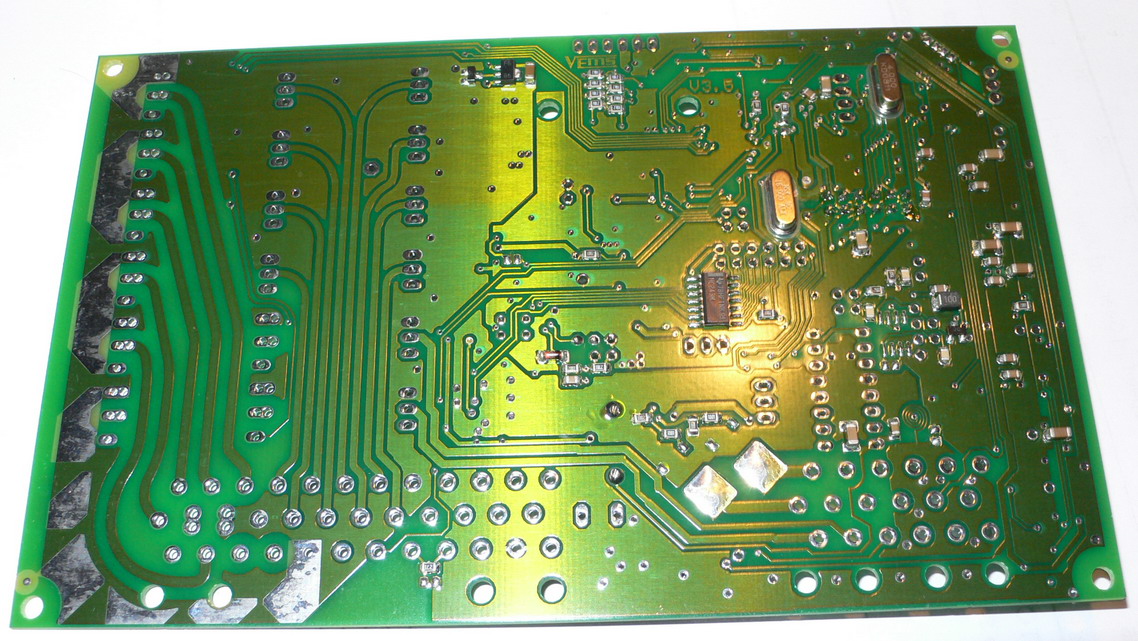
Some stuff which is not common to factory installs: * I'm using external dual-voltage flyback circuit (for much better injector control), so internally the low-voltage flyback is simply connected to EC36pin23 * I'm using pin headers instead of soldered wires, this makes servicing and disassembly neat * I'm using IRF640N FETs instead of the insulated FQPF20N06L drivers for injectors. These are necessary to survive my flyback. V3.5 bottom:
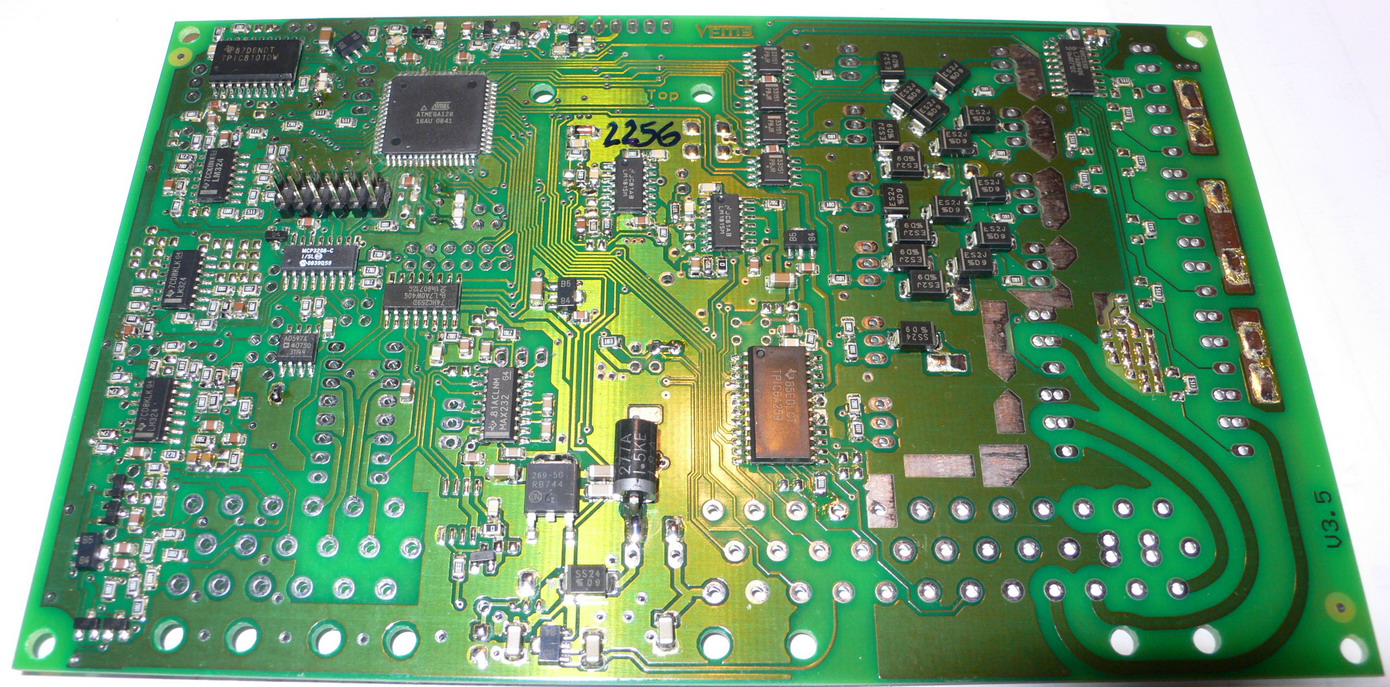
Top:
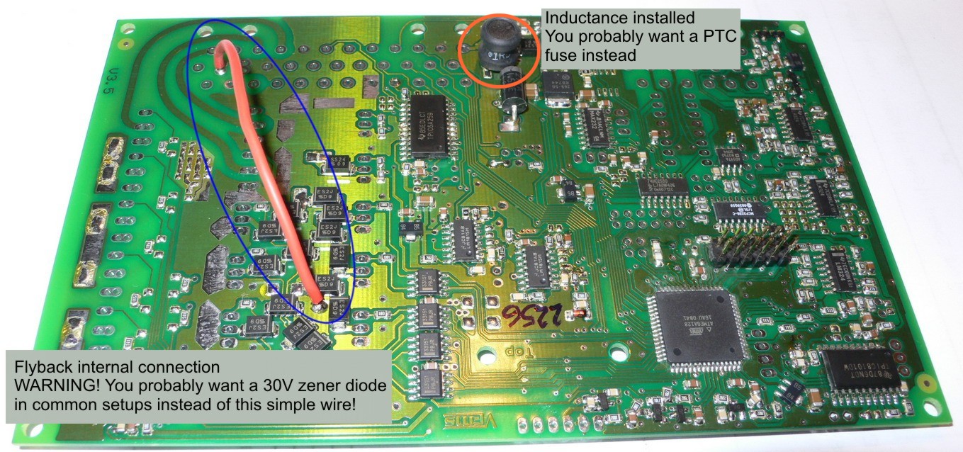
Internal flyback and supply-voltage inductance connected. I use external dual-voltage flyback (MembersPage/GergelyLezsak/FlyBack), that's why flyback connection is a simple wire here. With high-Z injectors or ballast resistors it is preferred to use a 30V zener diode here.
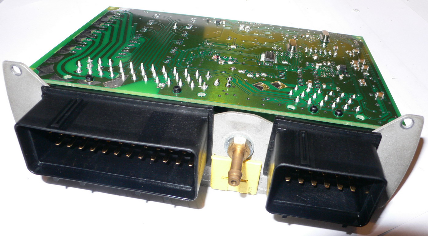
Econoseal-36 in place:
Frontplate fitted (hammered) to EC-36 to show the final position of EC-18:
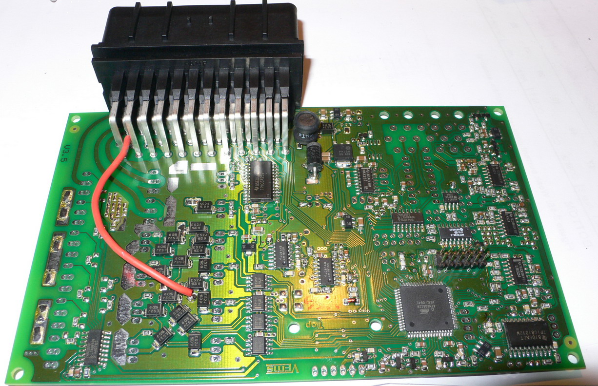
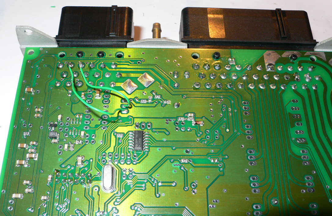
Both Econoseal connectors soldered and two bottom wires (green) of RS-232 serial connection. After this is done, the board is ready for a bench-powerup and communication test
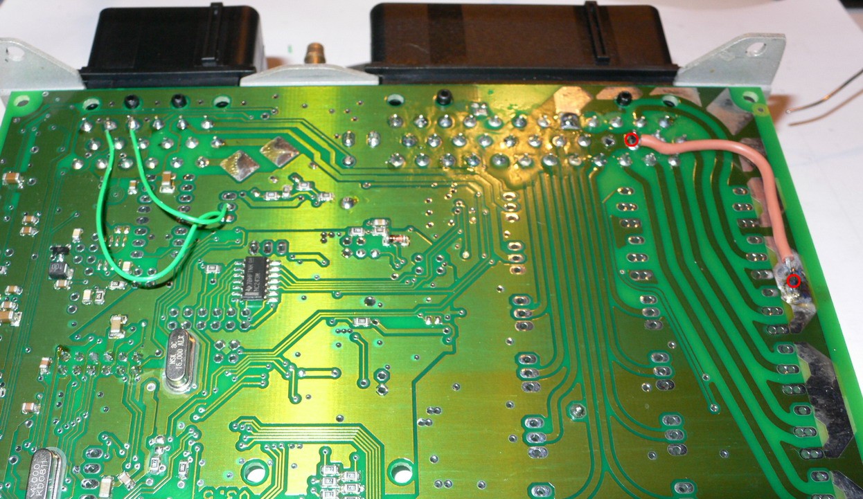
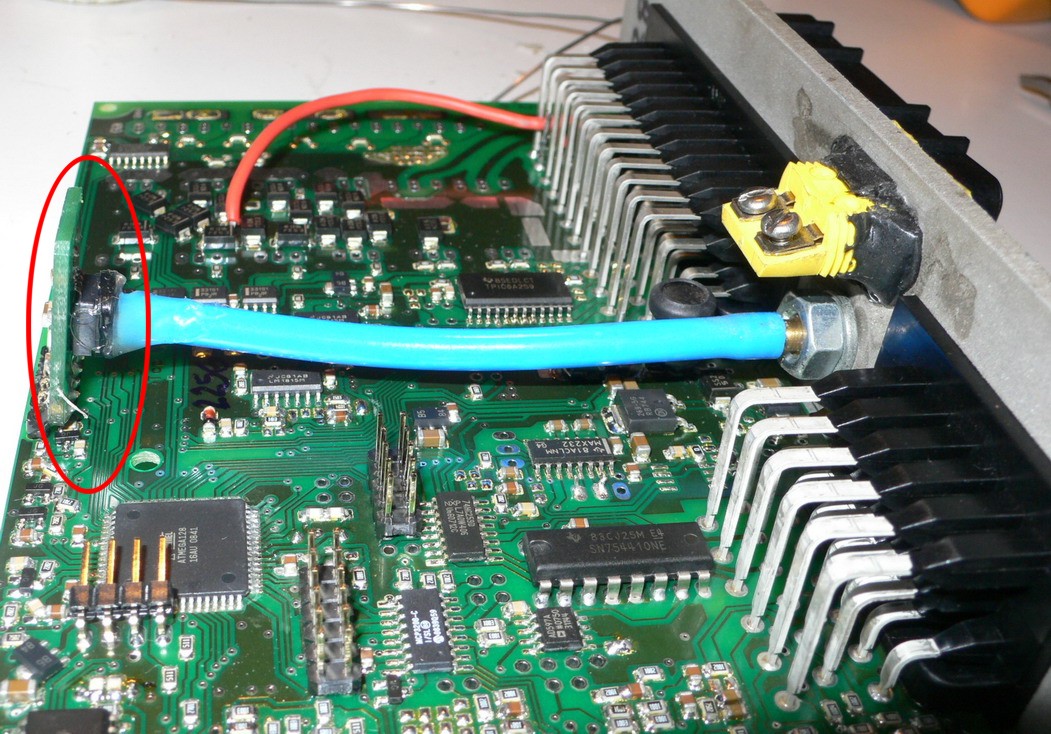
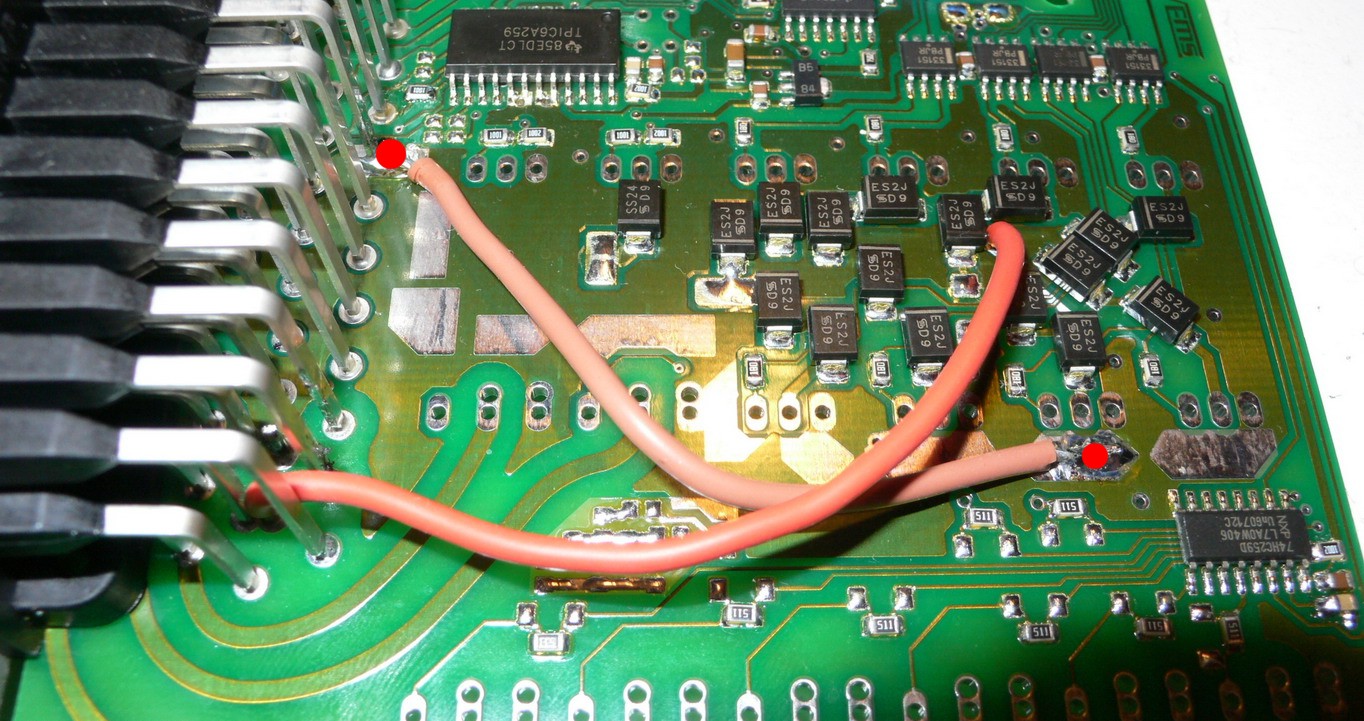
Ground reinforcement on the right side (pink wire, red circles)
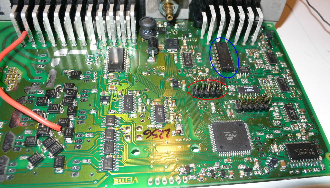
Stepper chip populated (blue oval) and pin headers for LCD (red oval)
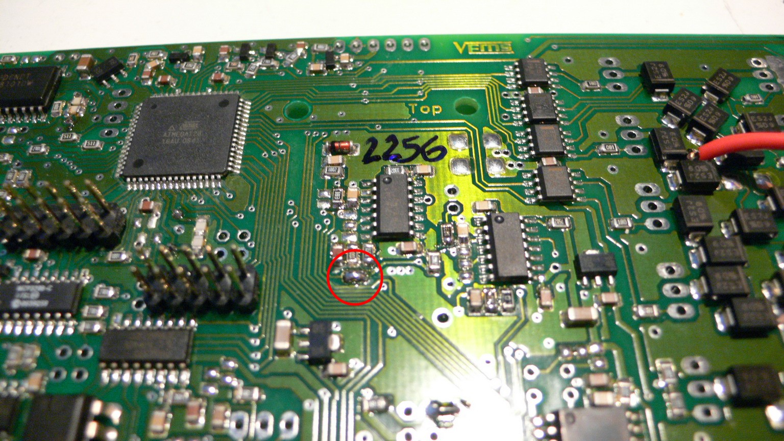
Solder-blob to enable primary VR chip:
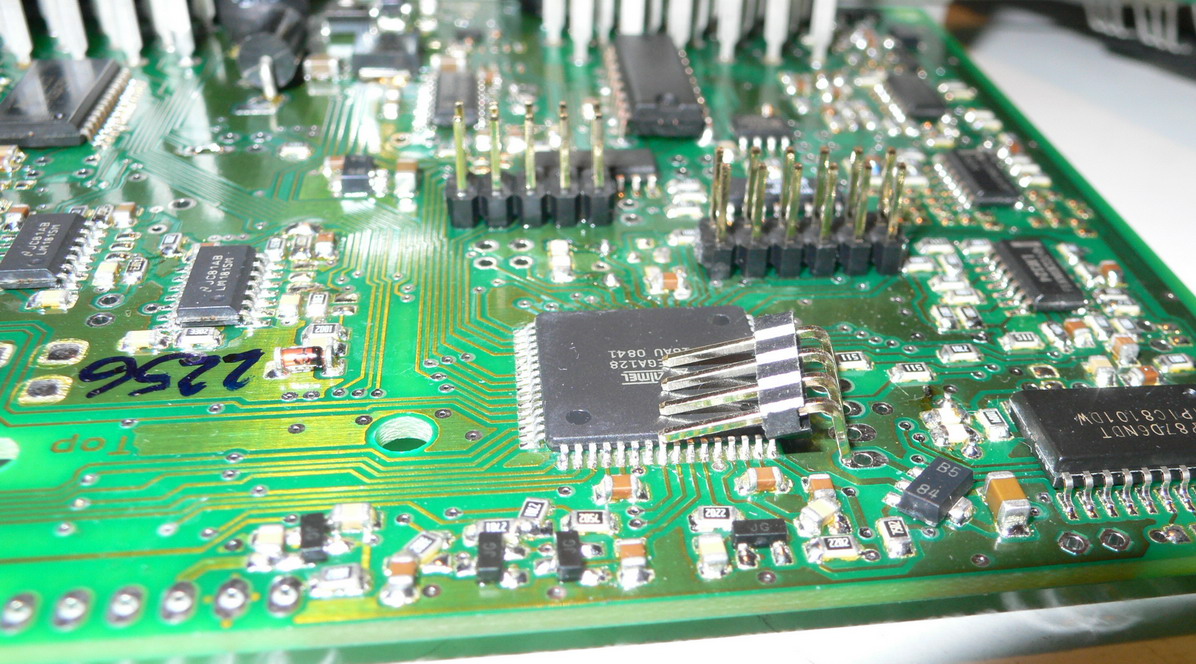
I'm going to use 90-deg. bent pin header for PS/2 keyboard input. It's just placed on top of the processor:
Bent PS/2 pin header soldered. This position will clear SDCard logger above
Internal MAP sensor board soldered and pneumatic tube connected:
Another GND reinforcement (red dots, pink wire):
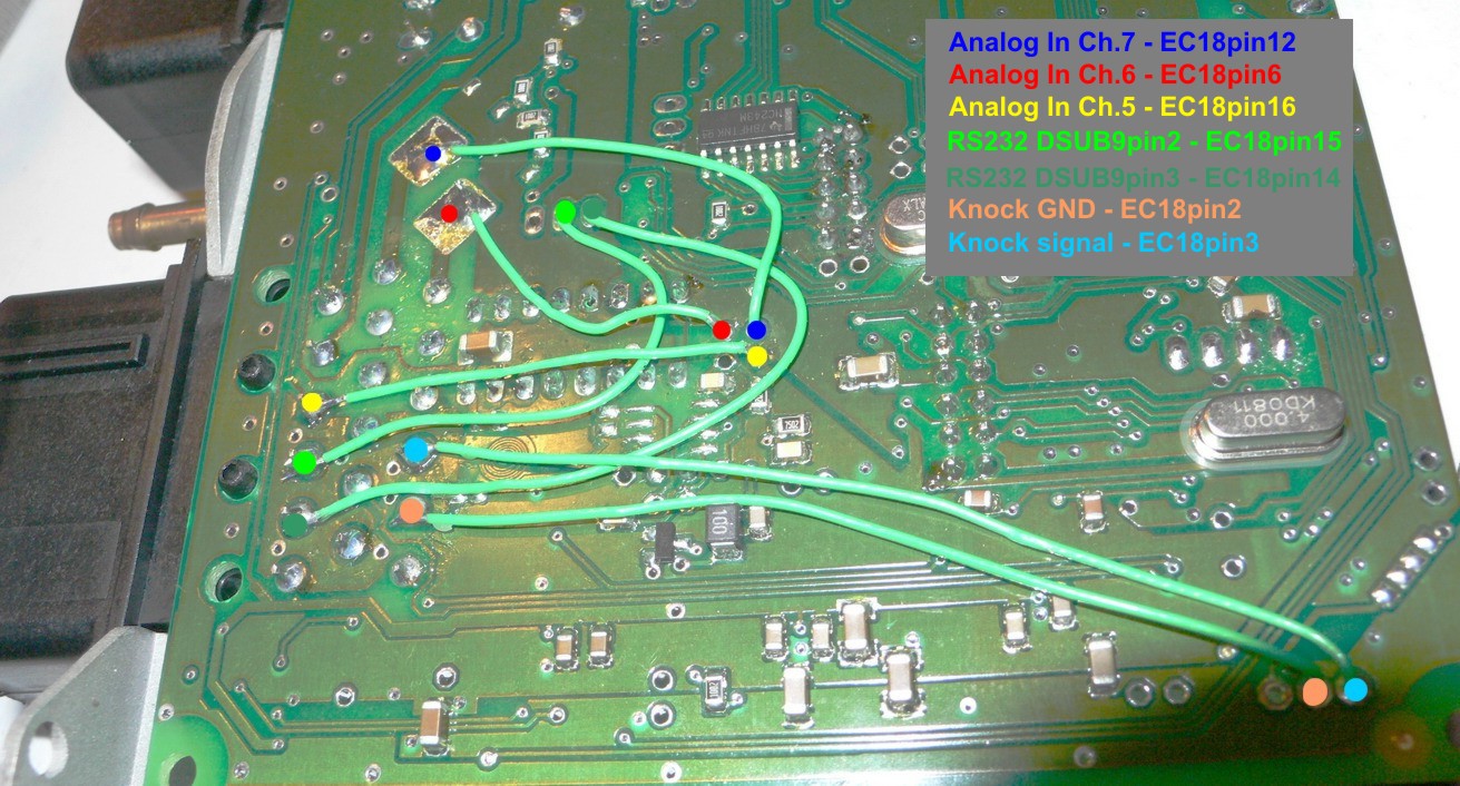
3 analog input channels and knock(1) connected to EC-18:
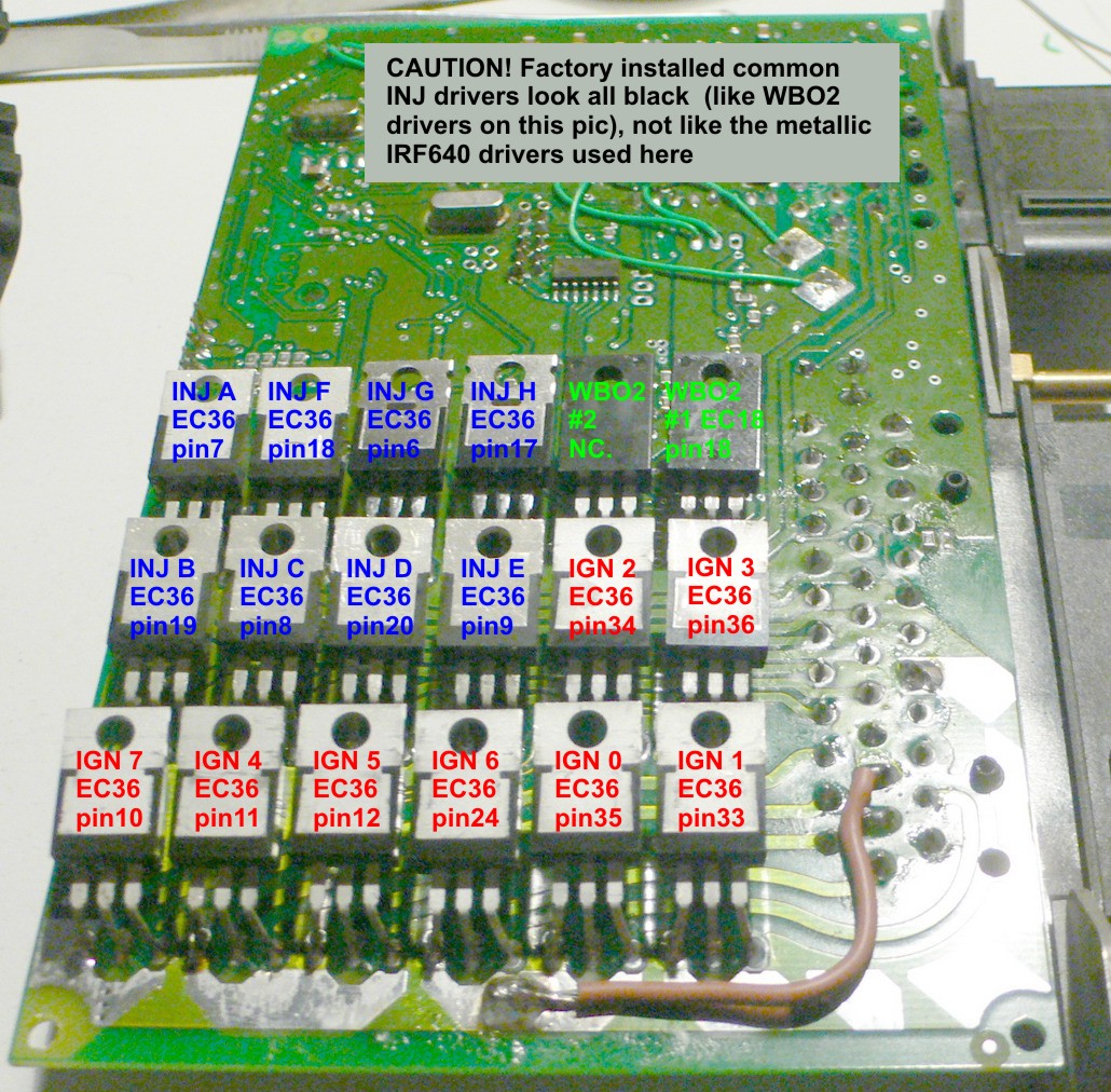
All the power drivers (FETs) installed here:
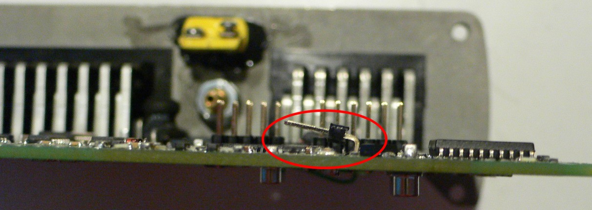
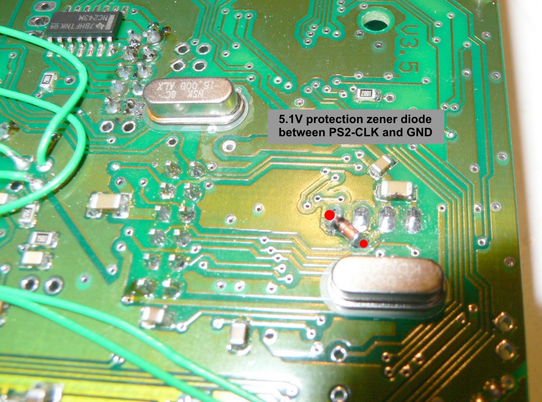
5v1 zener diode installed to PS2-pin header, to protect PS2/CLK pin, for wheelspeed input. Note that this SMD diode is originally not supposed to be here, I just found a ground nearby using a PCB through-hole
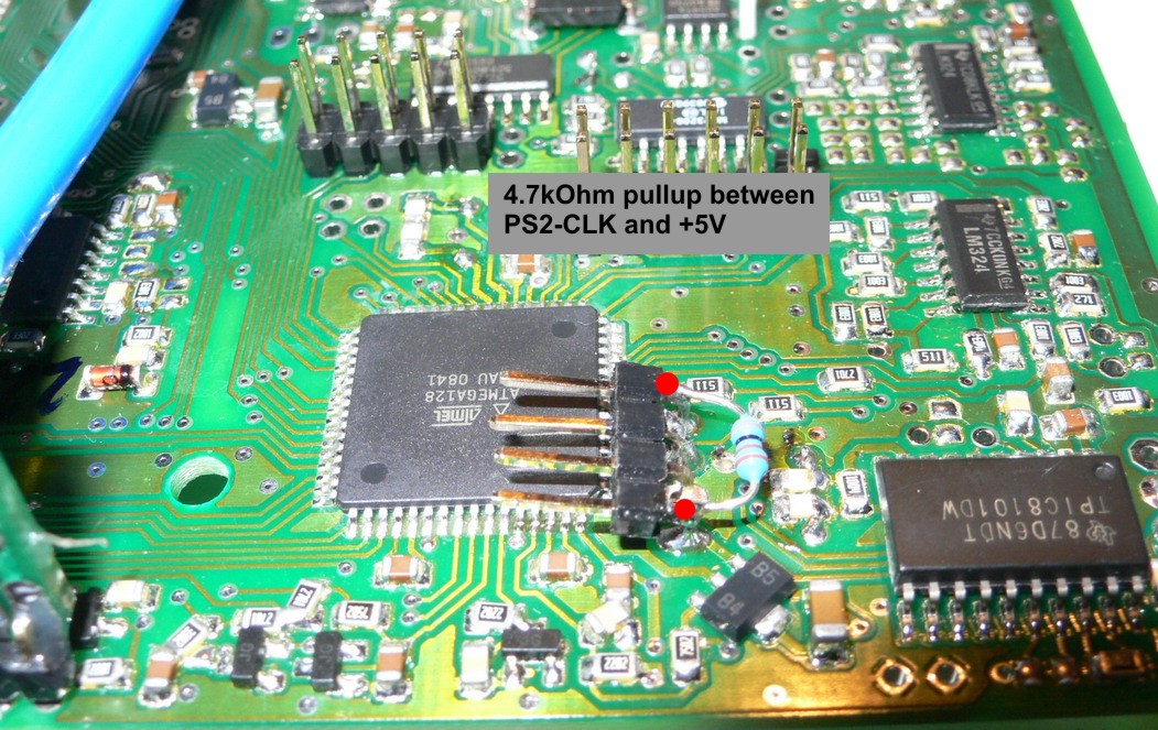
4.7k Ohm pullup resistor connected to +5V signal on pin-header
|